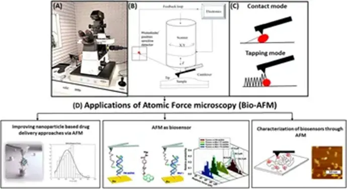
These two powerful analytical instruments are widely used in both industrial settings and university research labs: the Atomic Force Microscope (AFM) and the Confocal Raman Spectrometer (often called Confocal Raman Microscope). I’ll discuss each instrument’s principle, strengths, operational modes, key applications (industrial + academic), comparative considerations, and tips for implementation. If you like, I can provide case studies or examples specific to a field you’re interested in (e.g., semiconductors, polymers, biotech).
Atomic Force Microscope (AFM)

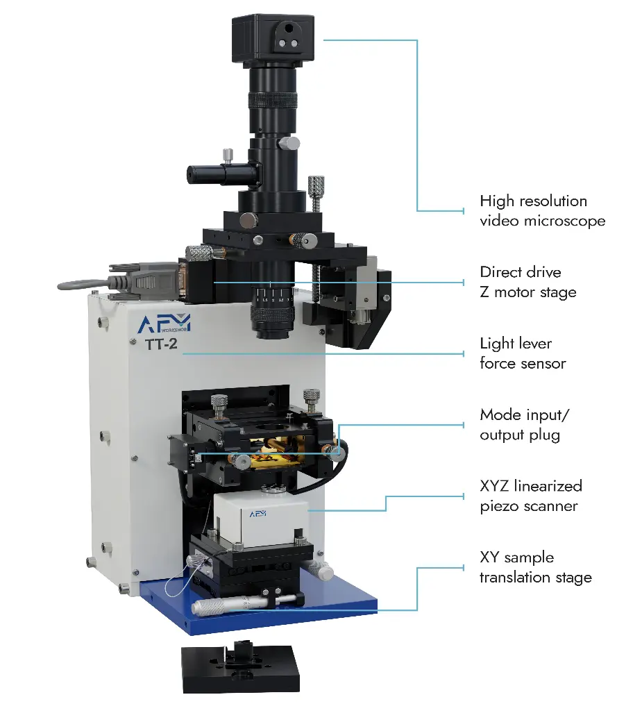
What is it & How does it work
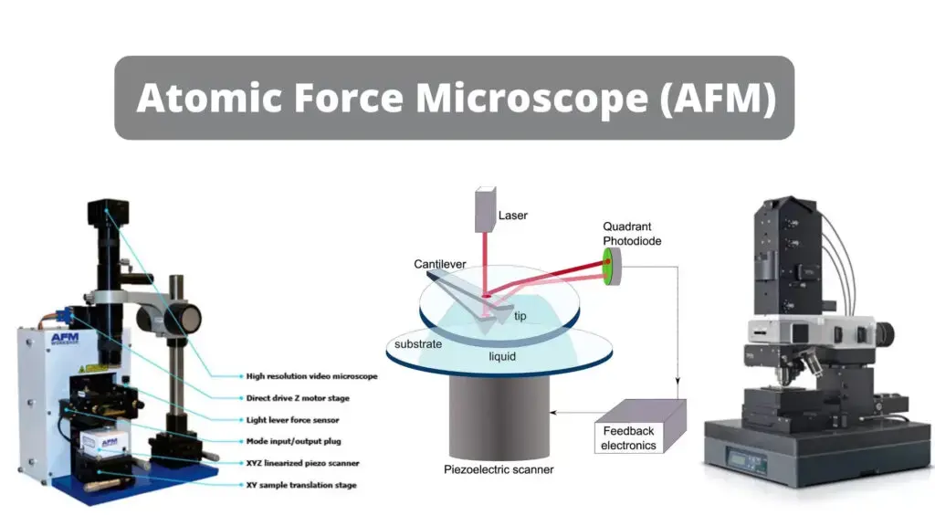
An Atomic Force Microscope (AFM) is a type of scanning probe microscope that produces high-resolution three-dimensional (3D) surface topography and also maps other surface properties at the nanoscale (down to fractions of a nanometre vertically).
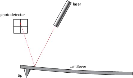
A very sharp tip (on the order of tens of nanometres or less) is mounted at the end of a flexible cantilever.
- The tip is moved (or the sample is moved) in a raster scan across the surface; the interaction forces (van der Waals, electrostatic, contact, etc) between tip and surface cause deflection or oscillation of the cantilever.
- A laser beam reflected off the back of the cantilever tracks its deflection, feeding into electronics that control a piezo-electric scanner to maintain a setpoint (constant force, constant height, constant amplitude) via feedback.
- From the feedback signal and/or the tip motion, we build up a 3D height map (and often additional property maps) of the surface.
Operating modes / modalities
AFM has several modes suited for different uses:
- Contact mode: Tip stays in continuous contact with surface—good for harder samples but risk of damage for soft ones.
- Tapping mode / intermittent contact: Cantilever oscillates and the tip contacts surface intermittently—minimizes lateral dragging; commonly used for soft or delicate samples.
- Non-contact mode: The tip hovers slightly above the surface and senses attractive forces—less common but used for ultra-soft or very delicate samples.
- Specialised modes: Lateral force microscopy (LFM), magnetic force microscopy (MFM), conductive AFM (C AFM), force spectroscopy (force-distance curves), nano mechanical mapping (elastic modulus, adhesion), phase imaging, etc.
Key strengths
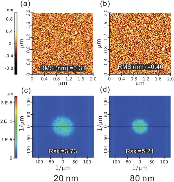
- Extremely high spatial resolution (even atomic for certain systems).
- Works for conductive and conductive samples. Unlike scanning tunnelling microscope (STM), AFM does not require conductivity.
- Can operate in air, vacuum or liquids—so biological/soft materials can be imaged in nearnative (hydrated) state.
- Provides not just topography but quantitative mechanical/adhesion/roughness/electrical property information if configured appropriately.
Applications in industrial & research labs
Industrial uses
- Surface roughness and texture control: In semiconductor wafer fabrication, thin film coatings (optics, displays), tribology (automotive components). E.g., checking trench shape/cleanliness, film uniformity.
- Coatings and thin films: Quality control in e.g. optical, hard coatings, MEMS (microelectromechanical systems).
- Material defects, wear, adhesion: In manufacturing of e.g. automotive tires, sport goods, hair-treatment products etc.
- Nanotechnology manufacturing: Characterizing nanowires, nanotubes, graphene, other nano structures used in electronics, sensors, composites.
- Bio/medical devices: Surface characterization of implants, stents, coatings, ensuring roughness/adhesion meets specifications.
University / research applications
- Nanomaterials research: Graphene, 2D materials, carbon nanotubes — examining morphology, step heights, defects, edges.
- Polymers & composites: Phase imaging of polymer blends, adhesion mapping between matrix/filler, wear studies.
- Biology / biomaterials: Imaging cells, membranes, proteins, DNA in liquids; measuring cell stiffness, adhesion, and mechanobiology.
- Fundamental surface science: Force spectroscopy to explore molecular interactions, single molecule stretching, Van der Waals/Casimir forces.
Practical considerations & tips
- Vibration/isolation: AFM is very sensitive; external vibration, acoustic noise, thermal drift can degrade performance.
- Sharp tip & calibration: Tip radius, spring constant, cantilever calibration matter for good quantitative data (especially force mode).
- Sample preparation and mounting: The sample must be well fixed, flat (for best results), and appropriate for the mode (hard vs soft).
- Choose right mode: For soft biological samples use tapping mode; for hard crystalline surfaces contact may suffice.
- Interpretation caution: Artifacts (tip convolution, feedback lag, adhesion artefacts) are common; user training matters.
- Throughput: Scanning is relatively slow compared to e.g. optical microscopy; for large surfaces or many samples plan time accordingly.
- Data richness vs complexity: The additional property maps (mechanical, electrical) are powerful but require calibration and sometimes custom analysis.
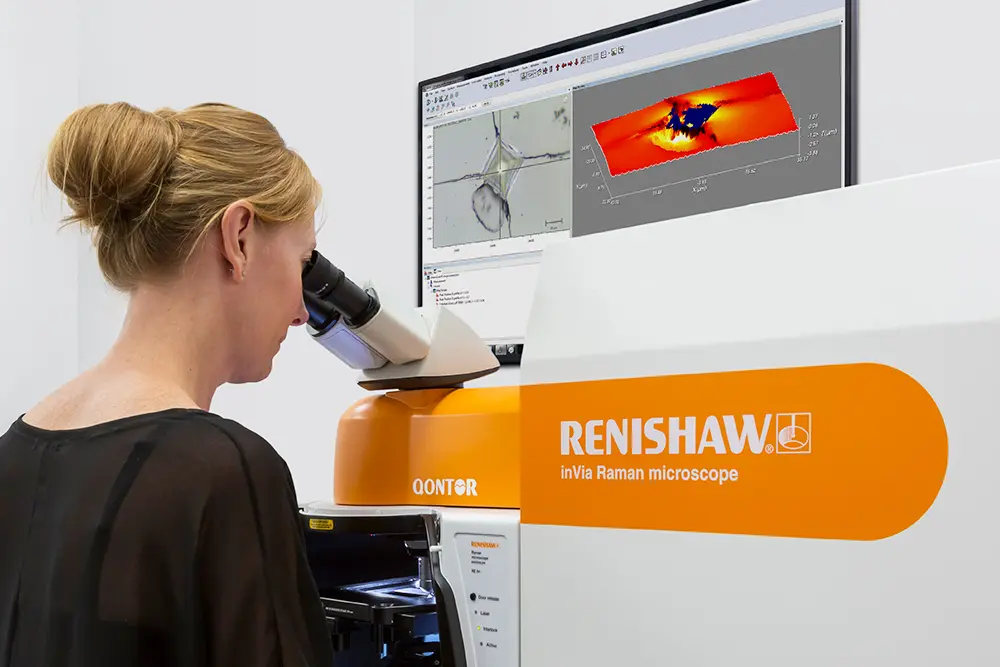
Confocal Raman Spectrometer / Microscope
What is it & How does it work
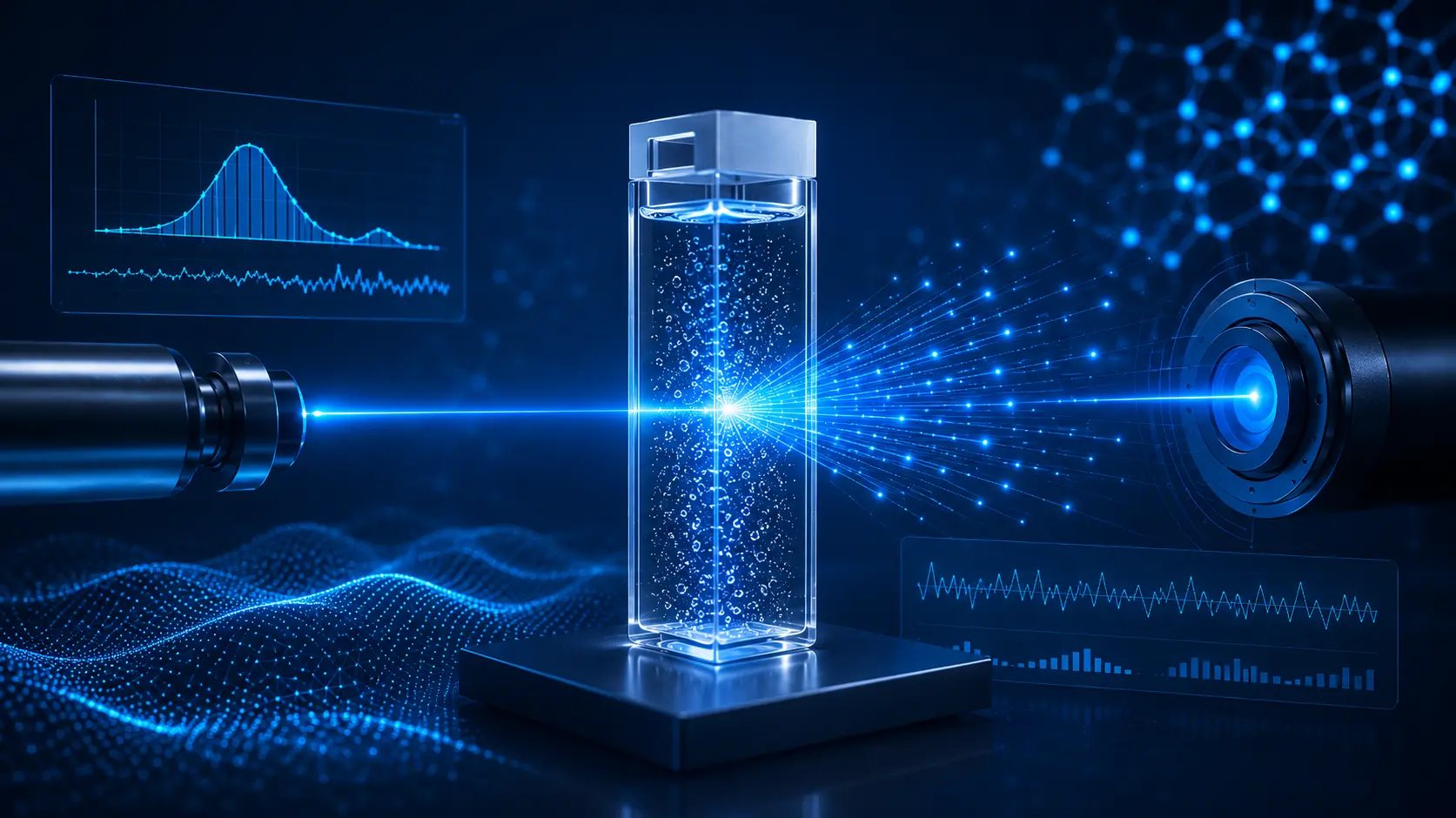
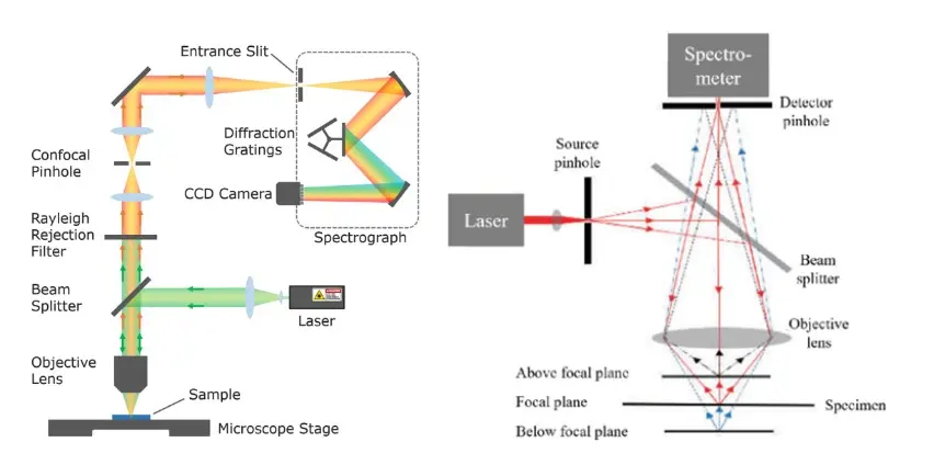
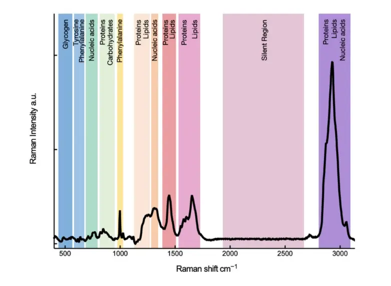
Raman spectroscopy is a vibrational spectroscopic technique based on inelastic scattering of monochromatic light (usually a laser) by molecules in a sample. The scattered light has slightly different energy (“Raman shift”) corresponding to vibrational (or rotational) modes of the molecules.
In a confocal Raman microscope, the Raman spectrometer is coupled to a microscope with confocal optics, allowing spatially resolved Raman spectra to be collected from small volumes (microns and below), thus enabling chemical imaging or mapping. Typical operation: A laser illuminates a small area → scattered light is collected via a spectrometer + detector → generate a Raman spectrum (a “molecular fingerprint”) → optionally perform point mapping or full imaging across the sample to map chemical distribution.
What’s special / advantages
- Chemical specificity: Raman spectrum acts like a fingerprint for molecular bonds and structure – you can identify materials, phases, polymorphs.
- Minimal sample preparation: Often non-destructive, no need for dyes/stains, can work through transparent packaging or in aqueous environment.
- Spatial resolution: Thanks to confocal optics, you can map chemical variation across a surface (2D) or even through depth (3D) in certain cases.
- Versatility: Applicable to organics, inorganics, polymers, biological tissues, and nanomaterials. E.g., for trace analysis, contaminant identification, process monitoring.
Applications in industrial & research labs
Industrial uses
- Pharmaceuticals / drug manufacturing: Raw material identification, tablet formulation (mapping distribution of Active Pharmaceutical Ingredient vs excipients), polymorph detection, quality control, in-process monitoring.
- Materials & composites: Characterising polymers (curing, cross-linking), composites (matrix vs filler distribution), nanomaterials (graphene, CNTs) for defects, doping, stress/strain.
- Semiconductors & electronics: Crystal quality, strain mapping in silicon wafers/thin films, defect identification.
- Forensics / counterfeit detection / packaging: Non-invasive spectral analysis through transparent containers; e.g., verifying blister packs of tablets, detecting adulterants or counterfeit drugs.
- Environmental & food / beverage / coatings: Contaminant detection, polymer degradation, quality control in food & packaging. University / research applications
- Chemical imaging / mapping: For example mapping distribution of APIs in tablets, or mapping multilayer polymer thin films.
- Nanomaterial characterisation: Graphene layer number, doping, defects via Raman features; carbon nanotubes via radial breathing mode.
- Biological / biomedical research: Label-free imaging of cells, tissues, biomolecules; studying chemical changes in situ, live cell imaging.
- Fundamental spectroscopy / materials science: Phase transitions, polymorphism, stress/strain in crystals, thin films.
- Practical considerations & tips
- Laser wavelength / power: Choose appropriately (e.g. avoid fluorescence issues; choose penetration depth vs resolution trade-off).
- Sample fluorescence: Some samples fluoresce under lasers, which can swamp Raman signal pre-testing and possibly use longer wavelength lasers may help.
- Spatial resolution vs scanning time: High resolution maps require more time; plan time budget accordingly.
- Confocal optics & depth: For true 3D chemical maps, need good confocal set up, stable focusing, and proper sample thickness.
- Calibration / standardization: For quantitative or comparative work (polymorph quantification, process control), ensure instrument calibration, spectral reproducibility.
- Data interpretation & chemometrics: Raman spectral datasets (especially mapping) can be large; advanced statistical methods/chemometrics often help.
- Cost / integration overhead: While highly versatile, Raman microscopes (especially confocal imaging/mapping variants) can have high capital and operational costs; for industrial in-line use cost-benefit must be established.
Comparing AFM vs Confocal Raman – when to use which (or both)
| Feature | AFM | Confocal Raman |
| Primary information | Surface topography + local physical/mechanical/electrical properties | Chemical composition, molecular structure, spatial mapping of chemical species |
| Scale / resolution | Vertical resolution down to <1 Å; lateral resolution ~nm range | Spatial resolution ~µm to sub µm (depending on optics); molecular resolution in spectroscopy rather than atomic imaging |
| Sample types | Any (conductive or non-conductive), hard or soft, even liquids | Many types (organics/inorganics/biological) but less ideal for very rough surfaces or metals with strong fluorescence/absorption |
| Destructive vs non-destructive | Non-destructive in most modes (especially non-contact) but tip can damage soft samples | Generally non-destructive, no sample staining needed; can probe through packaging in some cases |
| Industrial relevance | Surface/roughness/defect control, wear/tribology, nanofabrication QC | Chemical QC, formulation mapping, process monitoring, materials/composition control |
| Throughput / ease | Scanning is relatively slow; preparation and expertise needed | Point measurements fast; mapping slower; relatively user-friendly for standard tasks |
| Complementarity | AFM gives physical structure; Raman gives chemical identity. Combining gives richer insight (e.g., structure + chemistry). |
In many advanced labs the two techniques are complementary: for example one might use AFM to see the nanoscale morphology of a polymer blend, and then use Raman mapping to identify chemical domains in the same sample. Some systems even integrate the two (see micro Raman + AFM combinations) for correlative topography + chemical imaging.
Implementation in Research/Industrial Lab – Best Practices
- Define your measurement goals: Are you interested in surface morphology, mechanical properties, or chemical composition (or combination)? This drives choice of instrument/mode.
- Sample preparation & handling: Especially important for AFM (flatness, cleanliness) and for Raman (avoiding fluorescence, ensuring optical access).
- Instrument environment: For AFM, use vibration isolation table, acoustic enclosure. For Raman microscopy, ensure optical alignment, calibration of laser and detector, proper environmental control if required (e.g., microscopy of live cells).
- Training & user competence: Both techniques require skilled users to interpret data correctly (artifacts, tip convolution, calibration, spectral interpretation).
- Calibration & standards: Use known standards to check resolution, tip sharpness (AFM), spectral calibration (Raman) and mapping reproducibility.
- Data management: For Raman mapping, generate large datasets; appropriate software and data storage/analysis strategy is important. For AFM, many channels and large high-resolution scans can be heavy.
- Maintenance & consumables: AFM tips wear/damage, cantilevers need replacement; Raman lasers and optics require upkeep and sometimes alignment.
- Integration into workflow: For industrial labs especially, consider throughput, automation, integration with process control/quality systems, cost of analyses per sample/time.
- Reporting & interpretation: For industrial QC, robust protocols, acceptance criteria, documentation. For academic research, designing experiments, control samples, replicates, statistical analysis is key.
- Cross-validation / complementary methods: Often combining AFM + Raman (or with other techniques like SEM, TEM, XRD, etc) gives better insight.
Why These Tools Are Valuable in Today’s Labs
- The push for nanoscale engineering, advanced materials, miniaturisation, and complex multi-phase systems means tools that can probe at very fine scale are increasingly required. AFM addresses the morphology/property side, while confocal Raman addresses the chemistry/phase side.
- Many industrial and academic problems today are not just about “what is the shape” but “what is the chemical nature” and“how does shape/chemistry translate into performance”. For example, in a polymer composite, where are the filler particles, what is their chemistry, how do they interact with the matrix, what is the local roughness or adhesion?
- Non-destructive, minimal sample preparation methods reduce cost and increase throughput (especially for Raman). For delicate biological or soft materials, the ability to image in liquid (AFM) or aqueous environment (Raman) is a big plus.
- Advanced mapping/imaging capabilities (e.g., Raman chemical maps or AFM nano-mechanical maps) support modern research approaches of heterogeneous materials(not just homogeneous bulk) – critical in fields like biomaterials, energy materials (batteries/solar), and nanocomposites.
- As instrumentation improves (faster scan speeds, better detectors, automation, improved software), these tools become more accessible and integrated into routine workflows – both in universities and industry.
Challenges / Limitations to Be Aware Of
- Cost & complexity: Both AFM and confocal Raman systems are relatively high capital cost, require skilled operators, and may have maintenance overhead.
- Throughput limitations: AFM in particular, is slow compared to conventional optical microscopy; Raman mapping can take significant time for large areas at high resolution.
- Artifacts and misinterpretation: AFM can suffer from tip convolution, feedback errors, sample damage; Raman may suffer from fluorescence, background, poor signal for some samples, laser-induced heating.
- Sample suitability: Very rough or steep surfaces may be difficult for AFM; highly fluorescent or opaque samples may challenge Raman. In industrial QC, the robustness and reproducibility of results under production conditions must be validated.
- Training & skills: Without proper training, results may be misleading; e.g., in AFM, many users may image but misinterpret features (tip artefacts) or fail to calibrate; in Raman, mapping data may be huge and require chemometrics, which users may not be familiar with.
- Integration into industrial workflows: For industry, the instrument must meet cost benefit, speed, and automation demands; sometimes simpler techniques may deliver “good enough” results at lower cost.
Summary
In summary:
- The AFM is a highly capable tool for topography + physical/mechanical/electrical property mapping at the nanoscale. It is invaluable in nanoscale research, surface science, and industrial QC of surfaces/coatings/nanomaterials.
- The Confocal Raman Microscope is a powerful instrument for chemical/molecular composition imaging with spatial resolution, useful across many fields (pharmaceuticals, materials, semiconductors, biology).
- Together, or used in parallel, they provide a powerful complementary toolkit: morphological/physical data + chemical/structural data.
- For university research labs, both provide deep insight into advanced materials and biological systems. For industrial labs, they support quality control, process monitoring, failure analysis, and advanced material development – but require careful consideration of cost, throughput, integration, and user competence.
General FAQs (AFM and Raman)
- What is the main difference between Atomic Force Microscopy (AFM) and Confocal Raman Spectroscopy?
AFM measures surface topography and physical properties at the nanoscale, while Confocal Raman provides chemical composition and molecular structure information using light scattering. - Can AFM and Raman be used together?
Yes! They’re complementary—AFM gives physical structure and mechanical properties, Raman gives chemical identity. Some instruments even combine both for correlated imaging. - Which technique offers higher spatial resolution?
AFM offers higher spatial resolution(nanometre or even atomic scale). Raman is typically limited to sub-micron resolution due to the diffraction limit of light. - Are these techniques destructive to the sample?
Both are generally non-destructive, especially under standard conditions. However, improper AFM settings or high Raman laser power can damage soft or sensitive samples.
Atomic Force Microscope (AFM) FAQs
- What kinds of samples can be analyzed with AFM?
AFM can analyze almost any solid sample: hard (metals, ceramics), soft (polymers, gels), biological (cells, proteins), and even surfaces submerged in liquid. - What are the main operating modes of AFM?
Key modes include:
- Contact Mode(direct contact),
- Tapping/Intermittent Mode(reduced damage),
- Non-Contact Mode(ultra-sensitive),
- Specialized modes like Conductive AFM, Magnetic Force Microscopy (MFM), and Force Spectroscopy.
- What are the limitations of AFM?
- Slow scanning speed
- Small scan areas
- Tip-related artifacts
- Requires vibration isolation and careful sample preparation
- Can AFM measure material properties like stiffness or adhesion?
Yes. AFM can map mechanical properties such as Young’s modulus, surface adhesion, friction, and electrical conductivity depending on the tip and mode. - Is AFM imaging possible in liquid environments?
Absolutely. AFM can operate in liquids, making it suitable for imaging biological samples like live cells or proteins in near-physiological conditions. - What affects AFM image resolution the most?
- Tip sharpness
- Feedback control settings
- Vibration/noise
- Sample flatness and cleanliness
Confocal Raman Spectroscopy FAQs
- What kind of information does Raman spectroscopy provide?
Raman provides a molecular fingerprint—information about chemical bonds, crystal structure, stress/strain, polymorphs, and molecular orientation. - Can Raman spectroscopy identify unknown materials?
Yes. By comparing the Raman spectrum to reference databases, you can identify unknown compounds, contaminants, or phases. - What is “confocal” in Confocal Raman Microscopy?
“Confocal” means that light is collected only from a narrow depth range, enabling depth sectioning, better spatial resolution, and reduced background noise. - Can Raman spectroscopy detect polymers or biological molecules?
Yes. Raman is well-suited for polymers, pharmaceuticals, biomolecules, and even living cells without labels or dyes. - What are the main limitations of Raman spectroscopy?
- Weak signal(Raman scattering is rare)
- Fluorescence interference
- Sample heating with high laser power
- Poor performance with dark or rough metal surfaces
- Is Raman spectroscopy affected by sample color?
Yes. Dark or opaque samples can absorb laser light, leading to heating or fluorescence. Laser wavelength choice helps mitigate this. - Can Raman spectroscopy be used for 3D imaging?
Yes, with confocal Raman, you can generate 3D chemical maps by scanning through layers (depth profiling). - How do you choose the right laser for Raman spectroscopy?
Depends on:
- Fluorescence avoidance(use longer wavelengths like 785 nm)
- Penetration depth
- Resolution(shorter wavelengths like 532 nm offer better spatial resolution)
Applications & Industry Use FAQs
- Where are AFM and Raman spectroscopy commonly used in industry?
- AFM: Semiconductor surface QC, nanomaterial analysis, wear/friction studies, polymer interfaces
- Raman: Pharmaceutical formulation QC, counterfeit drug detection, graphene/2D materials analysis, stress mapping in wafers
- Which technique is better for quality control (QC) in manufacturing?
Depends on the target parameter:
- Use AFM for surface roughness, film thickness, wear
- Use Raman for chemical identification, impurity detection, or polymorph verification
Contact :
- Mobile/WhatsApp: +971526191767
- Email: sales@apex-instrument.com